

描述
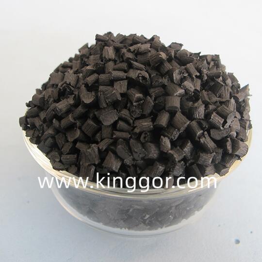
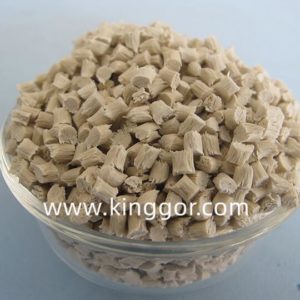
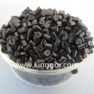
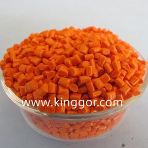
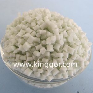
半导体材料PEEK颗粒
半导体材料PEEK颗粒
PEEK CF/GF30%颗粒,
聚醚醚酮树脂塑料,
任何颜色可供选择,
优点高抗冲击性,易于成型,
玻璃纤维增强碳纤维增强,
阻燃级,增韧级,
包装25kg/袋(也可定制)
半导体材料PEEK颗粒
产品详细信息
| 材质 |
半导体材料聚醚醚酮颗粒Modle |
半导体材料聚醚醚酮颗粒
在半导体行业,为了实现高功能性和低成本,硅片需要更大的尺寸和更先进的制造技术。低粉尘、低气体排放、低离子溶解和低吸水率对于半导体制造过程中的各种设备材料至关重要。特殊要求,这将是PEEK树脂展示才华的地方
立即联系:特蕾西
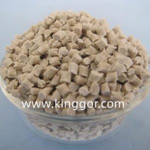
Semiconductor Material PEEK Granules
Semiconductor material PEEK granules
PEEK CF/GF30% pellets,
polyetheretherketone resin plastic,
Any color is available,
Advantage High impact resistance, easily molding,
Galss fiber reinforced carbon fiber reinforced,
Fire retardant grade, toughen grade,
Packing 25kg/bag(also customizable).
Semiconductor Material PEEK Granules
Product Details
Material
Semiconductor material PEEK granules
Modle
KY-TR15001
Semiconductor material PEEK granules
Semiconductor manufacturing and electronic and electrical industries have become another growth point in the application of PEEK resin.
In the semiconductor industry, in order to achieve high functionality and low cost, silicon wafers are required to be larger in size and more advanced in manufacturing technology. Low dust, low gas emission, low ion dissolution, and low water absorption are essential for various equipment materials in the semiconductor manufacturing process. Special requirements,
This will be where PEEK resin will show its talents.
More detail ofSemiconductor material PEEK granules.Any interested in, pls kindly contact me.
Contact now:Tracy<###>
在半导体行业,为了实现高功能性和低成本,硅片需要更大的尺寸和更先进的制造技术。低粉尘、低气体排放、低离子溶解和低吸水率对于半导体制造过程中的各种设备材料至关重要。特殊要求,这将是PEEK树脂展示才华的地方
立即联系:特蕾西
Semiconductor Material PEEK Granules
Semiconductor material PEEK granules
PEEK CF/GF30% pellets,
polyetheretherketone resin plastic,
Any color is available,
Advantage High impact resistance, easily molding,
Galss fiber reinforced carbon fiber reinforced,
Fire retardant grade, toughen grade,
Packing 25kg/bag(also customizable).
Semiconductor Material PEEK Granules
Product Details
| Material |
Semiconductor material PEEK granules |
| Modle | KY-TR15001 |
Semiconductor material PEEK granules
Semiconductor manufacturing and electronic and electrical industries have become another growth point in the application of PEEK resin.
In the semiconductor industry, in order to achieve high functionality and low cost, silicon wafers are required to be larger in size and more advanced in manufacturing technology. Low dust, low gas emission, low ion dissolution, and low water absorption are essential for various equipment materials in the semiconductor manufacturing process. Special requirements,
This will be where PEEK resin will show its talents.
More detail ofSemiconductor material PEEK granules.Any interested in, pls kindly contact me.
Contact now:Tracy<###>


评价
目前还没有评价